TMAG5170 3D Hall-effect sensor
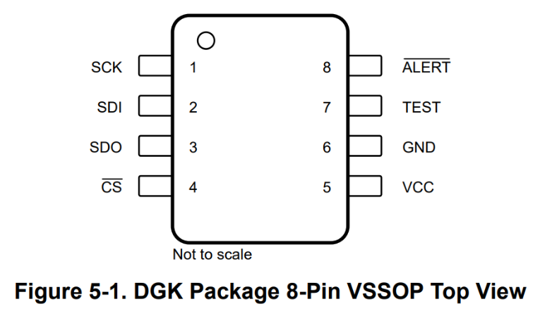
Pinout
TMAG5170 uses the standard 4-wire SPI. The clock rate on the SCK line can be up to 10 MHz.
The nALERT pin can be used as a trigger to start the conversion or as notification to signal the microcontroller to read the conversion result. A pull-up resistor should be connected to the nALERT pin, as it is an open-drain output.
The TEST pin should be grounded during normal operation.
A bypass capacitor must be placed between VCC and GND, or the high current demand during conversion may cause the device to brown out.
SPI communication
TMAG5170 uses a 32-bit SPI data frame. The first 28 bits are the data bits and the last 4 bits are CRC bits. TMAG5170 uses the polynomial and initial bits 0xff for CRC, see datasheet for more information.
SDI frame
The SDI frame is the 32-bit data frame sent from the microcontroller to the TMAG5170. The definition of the data bits are as follow:
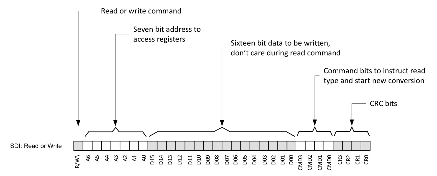
The most significant bit determines whether the command is a write(0) or read(1). The rest of the most significant byte is the address of the register to read from or write to. The middle 2 bytes are the data bits to write into the register. The upper nibble of the last byte is the command bits, which can be used to start a new conversion after the nCS line goes high.
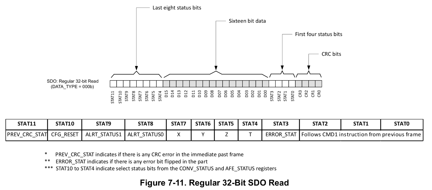
SDO frame
The SDO frame is the 32-bit data frame sent from the TMAG5170 back to the microcontroller. It contains 12 status bits and 16 data bits. The arrangement is shown in the following diagram.
CRC
CRC is used for error checking. If the TMAG5170 detects a CRC error in the SDI frame, it will invert the last bit of the SDO frame, making its CRC incorrect, to signal the microcontroller. TMAG5170 will not respond to register write commands if its CRC is incorrect. Also, the most significant bit of the SDO frame will go high if there is a CRC error in the previous frame.
CRC can be generated with linear shift registers. With our polynomial , XOR gates will be connected to the shift registers as shown in the following figure:
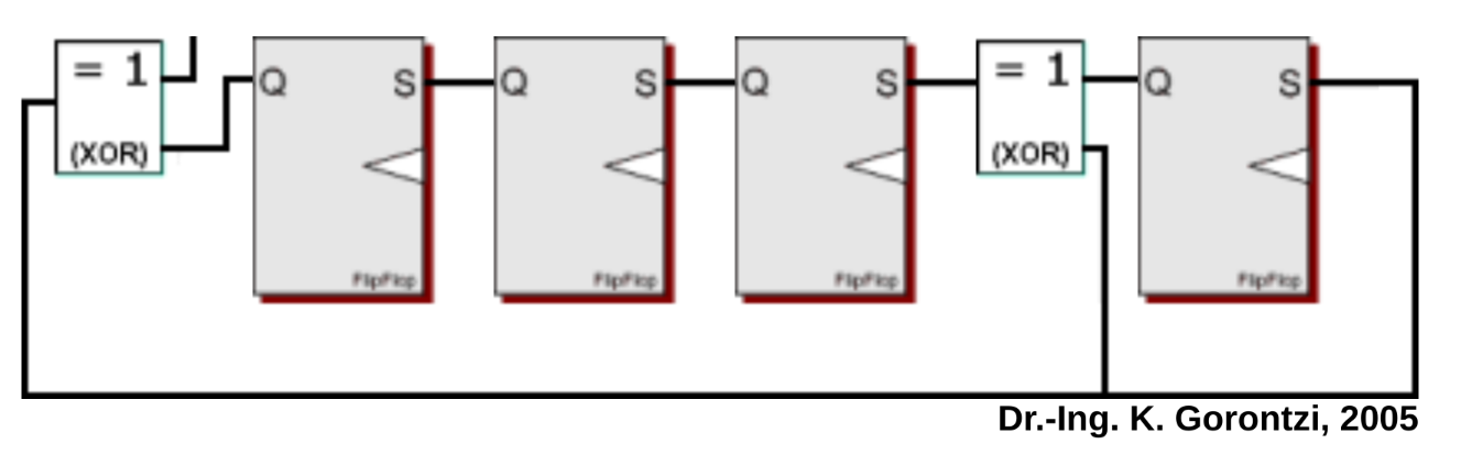
The 4 register will be initialised with the initial value 0b1111 and the 28 data bits will first be appended with 0's to 32 bits. After we shift all 32 bits into the shift register, the value in the 4 registers will be the CRC. The following listing shows the shift register implementation for CRC generation. The CRC can also be generated with 4 XOR functions shown in the datasheet.
uint32_t generateCRC(uint32_t data) {
    uint32_t CRC = 0xf;

    for(int i = 0; i < 32; i++) {
        uint32_t inv = ((data & 0x80000000) >> 31) ^ ((CRC & 0x8) >> 3);
        uint32_t poly = (inv << 1) | inv;
        uint32_t XORed = (CRC << 1) ^ poly;
        CRC = XORed & 0xf;
        data <<= 1;
    }

    return CRC;
}
Note that the data variable contains the data bits and is already padded with 0's.
Magnetic field conversion
Although there are 3 Hall-effect sensors on the TMAG5170, there is only 1 ADC. Thus, the conversion of the magnetic field on the 3 axes are done in a round robin fashion. Note that by "conversion" I mean the measurement of magnetic field. This terminology is used to stay consistent the datasheet.
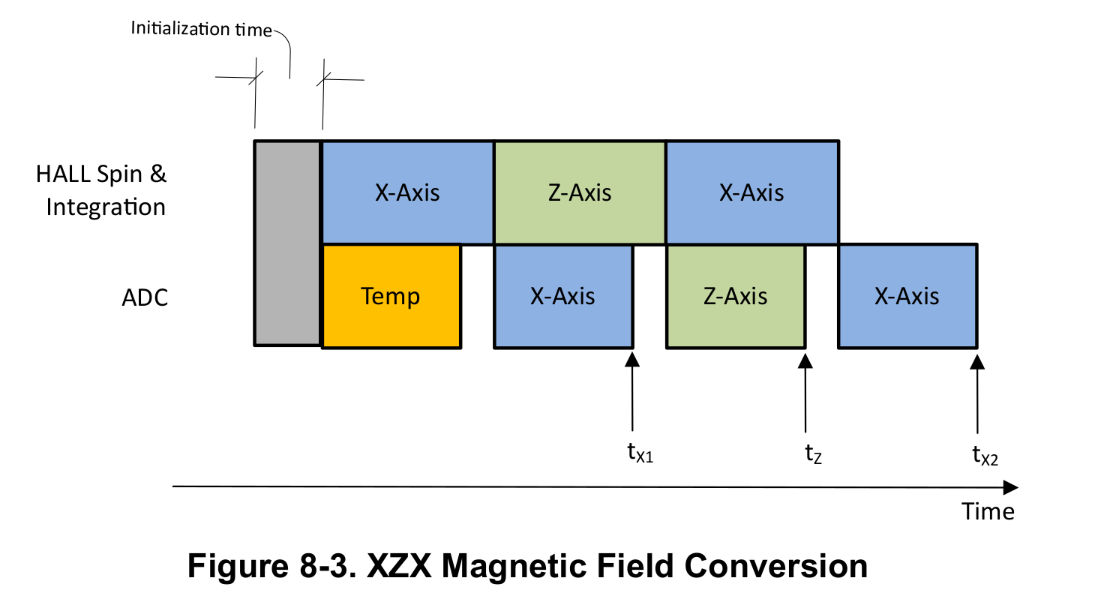 TMAG5170 measurement timing. (Source: Texas Instruments)
As shown in the figure, the measurements for the individual axes aren't performed simultaneously. This is called pseudo-simultaneous sampling. Pseudo-simultaneous sampling isn't a big issue when a lower sampling rate is used. As the difference in time between axes isn't significant compared to the sampling period. However, when the device is operated close to the maximum sampling rate, the effect of pseudo-simultaneous sampling should be considered.